Semiconductor for You
  • Home
  • Semiconductor News
  • Semiconductor Magazine
  • Technology
    • Automotive
    • Consumer Electronics
    • IoT
    • Test and Measurement
    • Lighting
    • Power Management
    • Wireless
    • Personal Electronics
    • Hardware & Software
    • Research
    • Medical Electronics
    • Embedded Design
    • Aerospace & Defence
    • Artificial Intelligence
  • Interview
  • Industries
  • Market
  • Knowledge Base
  • Events
  • Tools
    • Resistor Color Code Calculator
No Result
View All Result
  • Home
  • Semiconductor News
  • Semiconductor Magazine
  • Technology
    • Automotive
    • Consumer Electronics
    • IoT
    • Test and Measurement
    • Lighting
    • Power Management
    • Wireless
    • Personal Electronics
    • Hardware & Software
    • Research
    • Medical Electronics
    • Embedded Design
    • Aerospace & Defence
    • Artificial Intelligence
  • Interview
  • Industries
  • Market
  • Knowledge Base
  • Events
  • Tools
    • Resistor Color Code Calculator
No Result
View All Result
Semiconductor for You
No Result
View All Result
Home Semiconductor News

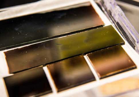
NREL develops scalable perovskite ink

Semiconductor For You by Semiconductor For You
April 19, 2017
in Semiconductor News
0
ADVERTISEMENT

Long processing window allows scalable production of thin films for high-efficiency solar cells
NREL develops scalable perovskite ink

Scientists at the US Department of Energy’s (DOE) National Renewable Energy Laboratory (NREL) have developed a new perovskite ink with a long processing window that allows the scalable production of perovskite thin films for high-efficiency solar cells.

ADVERTISEMENT

Proven highly efficient at converting sunlight into electricity, perovskite solar cells have yet to move beyond the laboratory.

The crystalline structure of perovskites must be carefully grown upon a substrate, which is normally done by laboratory-scale spin coating – a technology that can’t be scaled to large-scale manufacturing. The best devices fabricated using scalable deposition methods, which are suitable for future module production, still lag behind state-of-the-art spin-coated devices.

How the NREL scientists overcame this obstacle is spelled out in a new paper published in Nature Energy, ‘Perovskite ink with wide processing window for scalable high-efficiency solar cells’. Kai Zhu, a senior scientist in NREL’s Chemistry and Nanoscience Centre, is lead author. The co-authors are Mengjin Yang, Zhen Li, Matthew Reese, Obadiah Reid, Dong Hoe Kim, Sebastian Siol, Talysa Klein, Joseph Berry, and Michael van Hest from NREL, and Yanfa Yan from the University of Toledo.

To create a perovskite film, a coating of chemicals is deposited on a substrate and heated to fully crystalise the material. The various steps involved often overlap with each other and complicate the process.

One critical stage requires the addition of an antisolvent that extracts the precursor chemicals, and thus create crystals of good quality. The window for this step opens and closes within seconds, which is detrimental for manufacturing due to the precision required to make this time window.

NREL researchers were able to keep that window open as long as 8 minutes.

The formula for the precursor perovskite ink included a chlorine-containing methylammonium lead iodide precursor along with solvent tuning, coupled with an antisolvent, which could be deposited onto the substrate by either spin-coating or blade-coating methods. Both methods were tested and produced indistinguishable film morphology and device performance. Blade-coating is more attractive to manufacturers because it can easily be scaled up.

The researchers tested one precursor ink containing excess methylammonium iodide (MAI) and a second containing added methylammonium chloride (MACI). The MACI proved most effective in reducing the length of heat treatment the perovskites require, cutting the time to about a minute compared to  ten minutes for the MAI solution. The shorter time also should make the process more attractive to manufacturers.

Using blade-coated absorbers, NREL scientists made a four-cell perovskite module measuring about 12.6 cm2. Of that, 11.1cm2 were active in converting sunlight to energy and did so with a stabilised efficiency of 13.3 percent.

This research is supported by the DOE’s SunShot Initiative, a US national effort to drive down the cost of solar electricity and support solar adoption.

Semiconductor For You

Semiconductor For You

Browse by Category

  • Aerospace and Defence
  • AI & Data Center
  • Articles
  • Automation
  • Automotive
  • Communication
  • Consumer-Electronics
  • Design & Manufacturing
  • Hardware & Software
  • Industrial Electronics
  • Interview
  • IoT
  • Knowledge Base
  • Lighting
  • Market
  • personal-electronics
  • Power Management
  • Research
  • Semiconductor Events
  • Semiconductor News
  • Sensors
  • Technology
  • Test and Measurement
  • Uncategorized
  • Wireless
Semiconductor For You

Semiconductor For You is a resource hub for electronics engineers and industrialist. With its blend of
technology features, news and new product information, Semiconductor For You keeps designers and
managers up to date with the fastest moving industry in the world.

Follow Us

Browse by Category

  • Aerospace and Defence
  • AI & Data Center
  • Articles
  • Automation
  • Automotive
  • Communication
  • Consumer-Electronics
  • Design & Manufacturing
  • Hardware & Software
  • Industrial Electronics
  • Interview
  • IoT
  • Knowledge Base
  • Lighting
  • Market
  • personal-electronics
  • Power Management
  • Research
  • Semiconductor Events
  • Semiconductor News
  • Sensors
  • Technology
  • Test and Measurement
  • Uncategorized
  • Wireless

Recent News

Infineon introduces RIC70115 radiation-hardened GaN HEMT driver for satellite and high-reliability space applications

Infineon introduces RIC70115 radiation-hardened GaN HEMT driver for satellite and high-reliability space applications

July 16, 2026
Cabinet Approves Semicon 2.0 with ₹1.27 Lakh Crore Outlay to Power India’s Semiconductor Future

Cabinet Approves Semicon 2.0 with ₹1.27 Lakh Crore Outlay to Power India’s Semiconductor Future

July 15, 2026
  • About
  • Advertise
  • Privacy & Policy
  • Contact

© 2026 Semiconductor For You

No Result
View All Result
  • Home
  • Semiconductor News
  • Technology
    • IoT
    • Wireless
    • Power Management
    • Automotive
    • Hardware & Software
  • Market
  • Interview
  • Knowledge Base
  • Tools
    • Resistor Color Code Calculator

© 2026 Semiconductor For You

Advertisement