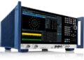
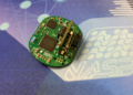
GlobalFoundries launches 8SW RF SOI process for next-gen mobile and 5G applications
GlobalFoundries of Santa Clara, CA, USA (one of the world’s largest semiconductor foundries, with more than 250 customers and operations...




GlobalFoundries of Santa Clara, CA, USA (one of the world’s largest semiconductor foundries, with more than 250 customers and operations...
Deposition equipment maker Aixtron SE of Herzogenrath, Germany has received an order for an AIX G5+ metal-organic chemical vapor deposition...
The Quad Small Form Factor Pluggable Double Density (QSFP-DD) Multi Source Agreement (MSA) group has released an updated 3.0 Hardware...
Tokyo-based Showa Denko K.K. (SDK) has decided to expand its facilities for producing high-quality-grade silicon carbide (SiC) epitaxial wafers for...
Deposition equipment maker Aixtron SE of Herzogenrath, near Aachen, Germany has received an order for multiple metal-organic chemical vapor deposition...
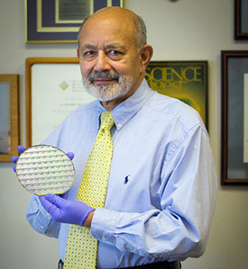
North Carolina State University (NCSU) is rolling out a new manufacturing process and chip design for silicon carbide (SiC) power...
Norstel AB of Norrköping, Sweden has developed low-defect-density 150mm silicon carbide (SiC) n-type substrates. Norstel manufactures conductive (n-type) and semi-insulating...
The 100G Lambda Multi-Source Agreement (MSA) Group has announced their intent to develop specifications based on 100Gbps per wavelength optical...
Evatec Ltd of Trübbach, Switzerland (which makes thin-film deposition and etch processing equipment for advanced packaging, power device, MEMS, optoelectronics,...
The Compound Semiconductor Centre (CSC) - a joint venture between Cardiff University and epiwafer foundry and substrate maker IQE plc...






Semiconductor For You is a resource hub for electronics engineers and industrialist. With its blend of
technology features, news and new product information, Semiconductor For You keeps designers and
managers up to date with the fastest moving industry in the world.