Towards gallium nitride integration with silicon CMOS
Researchers in the USA have developed gallium nitride (GaN) high-electron-mobility transistors (HEMTs) fabricated on 200mm-diameter silicon-on-insulator (SOI) substrates with multiple...

Researchers in the USA have developed gallium nitride (GaN) high-electron-mobility transistors (HEMTs) fabricated on 200mm-diameter silicon-on-insulator (SOI) substrates with multiple...
For first-half 2017, Riber S.A. of Bezons, France, which manufactures molecular beam epitaxy (MBE) systems as well as evaporation sources...
For fiscal third-quarter 2017 (to end-June), Skyworks Solutions Inc of Woburn, MA, USA (which manufactures analog and mixed-signal semiconductors) has...
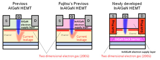
At the 12th International Conference on Nitride Semiconductors (ICNS-12) in Strasbourg, France (24-28 July), Tokyo-based Fujitsu Ltd and Fujitsu Laboratories...
Through the US Department of Energy’s SunShot Initiative Program (which to drive down the cost of solar electricity and support...
Semiconductor For You is a resource hub for electronics engineers and industrialist. With its blend of
technology features, news and new product information, Semiconductor For You keeps designers and
managers up to date with the fastest moving industry in the world.