New Geman Research Centre Will Focus On Graphene And 2D Materials
Aachen-based centre to bridge gap between science and applications within 2D materials based electronics and photonics RWTH Aachen University and...

Aachen-based centre to bridge gap between science and applications within 2D materials based electronics and photonics RWTH Aachen University and...

Woowon Technology will represent Oxford Instruments’ complete range of etch, deposition and growth solutions Oxford Instruments Plasma Technology has signed...

AIX 2800G4-TM planetary system will support market demand for infrared high power lasers and GaAs LEDs German deposition company Aixtron...
III-V optoelectronic foundry Compound Semiconductor Technologies Global Ltd (CST Global) of Hamilton International Technology Park, Blantyre, near Glasgow, Scotland, UK...
Pallidus Inc (a Melior Innovation company) of Houston, TX, USA has launched its proprietary M-SiC silicon carbide source material and...
Deposition equipment maker Aixtron SE of Herzogenrath, near Aachen, Germany says that Osram Opto Semiconductors GmbH of Regensburg, Germany has...
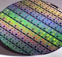
Commonly used semiconductor materials The example of semiconductor materials are germanium (Ge), silicon (Si), carbon (C), selenium (Se), gallium arsenide...
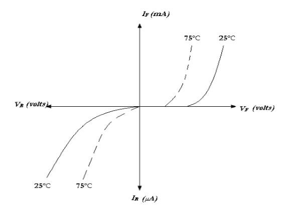
We have already discussed that, the current that a PN junction diode can conduct at a given voltage is dependent...

The optical transducer convert light into electrical quantity. They are also called as photoelectric transducers. The optical transducer can be...

Collaboration ensures research projects can be taken "seamlessly from the laboratory to commercial volume production", says Richard Hogg, professor of...
Semiconductor For You is a resource hub for electronics engineers and industrialist. With its blend of
technology features, news and new product information, Semiconductor For You keeps designers and
managers up to date with the fastest moving industry in the world.