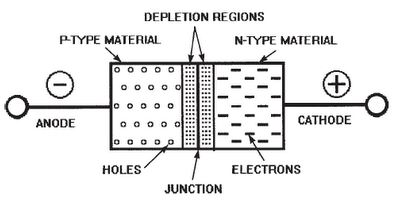
A P-type semiconductor is suitably joined to on N-type semiconductor under suitable condition by using a special technique to form a junction then the device constructed is a PN junction diode semiconductor diode.
The PN junction either in germanium or silicon crystal. It has two terminals i.e. one is anode and another is cathode. The P region of the PN junction diode is act as anode (A) and the N region of diode act as cathode (C).
The PN junction forms itself the most semiconductor device called semiconductor diode. The PN junction is represented by its symbol as shown in below figure. When it is forward biased the conventional current flow which is show by the arrow head shown in the symbol.
Construction of PN junction diode:

The PN junction diode consist of a PN junction formed either germanium or silicon crystal.
By joining of P-type semiconductor and N-type semiconductor the PN junction diode is formed using a special technique. It has two terminal anode and cathode.
The anode of a PN junction diode is connected across negative terminal of applied voltage and the cathode is connected across a positive terminal of voltage.
