• Home
  • About Us
  • Contact Us
Semiconductor for You
  • Home
  • Semiconductor News
  • Technology
    • Automotive
    • Consumer Electronics
    • IoT
    • Lighting
    • Power Management
    • Wireless
    • Personal Electronics
    • Hardware & Software
    • Research
    • Medical Electronics
    • Embedded Design
    • Aerospace & Defence
    • Artificial Intelligence
  • DIY Projects
  • Market
  • Industries
    • Renesas Electronics
  • Knowledge Base
  • Events
  • Tools
    • Resistor Color Code Calculator
No Result
View All Result
Semiconductor for You
No Result
View All Result
Home Articles

V-I characteristic of tunnel diode

Semiconductor For You by Semiconductor For You
July 17, 2017
in Articles
0
ADVERTISEMENT

The Tunnel diode is a highly doped semiconductor device which is commonly used for low voltage high frequency switching applications. It works on the principle of Tunneling effect.

It immediately conducts the diode when forward biased voltage is applied. The current is increases to its peak point value (Ip). The diode currents starts decreasing till it reaches its minimum value called valley point current (Iv) corresponding to valley voltage (Vv), when the forward voltage is increases.Current starts increasing again as in ordinary junction diode, for more voltage than valley voltage (Vv).

V-I characteristic of tunnel diode

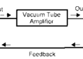
The region between point A and B is called negative resistance region. Current decreases with increase in applied voltage in negative resistance region that is tunnel diode possessing negative resistance region (Rn) in this region. Negative resistance of negative resistance region produces power instead of absorbing power. The negative resistance permits oscillations. So tunnel diode used as a very high frequency oscillator

Content Protection by DMCA.com
Tags: diodeSemiconductors
Semiconductor For You

Semiconductor For You

Browse by Category

  • Aerospace and Defence
  • Articles
  • Automotive
  • Consumer-Electronics
  • Hardware & Software
  • Interview
  • IoT
  • Knowledge Base
  • Lighting
  • Market
  • personal-electronics
  • Power Management
  • Research
  • Semiconductor Events
  • Semiconductor News
  • Technology
  • Wireless
Semiconductor for You

Semiconductor For You is a resource hub for electronics engineers and industrialist. With its blend of
technology features, news and new product information, Semiconductor For You keeps designers and
managers up to date with the fastest moving industry in the world.

Follow Us

Browse by Category

  • Aerospace and Defence
  • Articles
  • Automotive
  • Consumer-Electronics
  • Hardware & Software
  • Interview
  • IoT
  • Knowledge Base
  • Lighting
  • Market
  • personal-electronics
  • Power Management
  • Research
  • Semiconductor Events
  • Semiconductor News
  • Technology
  • Wireless

Recent News

New SPI Absolute Encoder Supports 9 mm to 15.875 mm Motor Shafts

New SPI Absolute Encoder Supports 9 mm to 15.875 mm Motor Shafts

June 11, 2025
Infineon Secures the Future with 10 Billion Integrity Guard Chips Delivered

Infineon Secures the Future with 10 Billion Integrity Guard Chips Delivered

June 11, 2025
  • About
  • Advertise
  • Privacy & Policy
  • Contact

© 2022 Semiconductor For You

No Result
View All Result
  • Home
  • Semiconductor News
  • Technology
    • IoT
    • Wireless
    • Power Management
    • Automotive
    • Hardware & Software
  • Market
  • Knowledge Base
  • Tools
    • Resistor Color Code Calculator

© 2022 Semiconductor For You