

- The 7400 series of TTL logic integrated circuits was introduced in October 1966 and they soon became the standard for all logic integrated circuits.
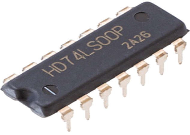
- IC 7400 is a fourteen-pin Logic Gate IC. The IC 7400 consist of four NAND Gates. The NAND Gate is also called Universal Gate. The NAND gate has a total of three terminals, two input terminals, and one output terminal. All NAND Gates are independent. IC 7400 is also called Quad 2-input NAND Gate IC.
- The 7400 logic series of ICs were fabricated using bipolar transistor technology and this gave its name to the logic technology, TTL standing for transistor-transistor logic.
- The 7400 series TTL ran from a nominal 5 Volt supply line and as a result of its popularity, the 5 V line became standard for logic chips for many years, only changing when power restrictions and smaller feature sizes on chips as a result of higher integration and new processes forced the operating voltage down.
- Although launched in the mid-1960s the 7400 series became the main standard set of logic widely used in electronic digital circuits. There were earlier TTL series of chips. Motorola launched a logic family with the trade name MTTL (Motorola Transistor-Transistor Logic), and other series were launched by national Semiconductor, Fairchild, and Signetics.
- With their increasing popularity, the cost of the chips came down. Initial offerings cost many dollars each, but over time as production techniques matured and quantities rose vastly, some 7400 series chips could be bought for a few cents each.

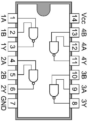
Pin Configuration

| Pin | Description |
|---|---|
| Pin 1 | It is connected to the Input(A) of NAND Gate 1 |
| Pin 2 | Input (B) of NAND Gate 1 |
| Pin 3 | It is connected to the Output(Y) of NAND Gate 1 |
| Pin 4 | Input (A) of NAND Gate 2 |
| Pin 5 | Input (B) of NAND Gate 2 |
| Pin 6 | This pin provides the Output (Y) of NAND Gate 2 |
| Pin 7 | Ground Pin which used to provide the power supply to the IC |
| Pin 8 | It is connected to the Output (Y) of NAND Gate 3 |
| Pin 9 | It is connected to the Input (A) of NAND Gate 3 |
| Pin 10 | Input (B) of NAND Gate 3 |
| Pin 11 | It is the output (Y) pin of the NAND Gate 4 |
| Pin 12 | It is the input (A) pin of the NAND Gate 4 |
| Pin 13 | It is the input (B) pin of the NAND Gate 4 |
| Pin 14 | It is a Vcc pin which used to provide the power supply to the IC |
Specifications of IC 7400
- The voltage supply is 5 V.
- Propagation delay for each gate will be 10 ns.
- Maximum toggle speed is 25 MHz.
- Power utilization for each gate is 10 mW.
- Independent 2-i/p NAND Gates- 4.
- The output can be interfaced with TTL, NMOS, or CMOS.
- The range of operating voltage will be large.
- Operating conditions are extensive.
- Not suitable for new designs which use 74LS00.
- Using 7400 family-based integrated circuits, an engineer can design flip-flops (FFs), counters, buffers, and logic gates in different packages, and these can be connected as preferred to solve an exact problem.
7400 Family IC’s
| Device Number | Description |
|---|---|
| 7400 | Quad 2-input NAND gate |
| 7402 | Quad 2-input NOR gate |
| 7404 | Hex Inverter |
| 7408 | Quad 2-input AND gate |
| 7432 | Quad two-input OR gates |
| 7447 | BCD to seven-segment display decoder/driver |
| 7474 | Dual D-type positive edge triggered flip-flops |
| 7470 | Four-bit decade counter |
| 7486 | Quad 2-input XOR gate |
| 7490 | Four-bit decade counter |
| 74138 | Three-to-eight decoder |
| 74153 | Dual 4-to-1 multiplexer |
| 74157 | Quad D-type flip-flops with complementary outputs |
| 74160 | Four-bit binary synchronous center |
| 74164 | Eight-bit parallel-out serial shift register |
| 74174 | Quad D-type flip flops with complementary outputs |
| 74193 | Four-bit synchronous up/down binary counter |
| 74245 | Octal bus transceiver with tri-state outputs |
| 74266 | Quad 2-input XNOR gate |
| 74373 | Octal D-type transparent latch |
| 74374 | Octal D-type flip-flops |
IC 7400, NAND Gate
- 7400 IC is the most widely used TTL (Transistor-Transistor Logic) device in the world. It contains four independent two-input NAND gates. Its popularity is based on the fact that any logic gate function can be created using only NAND gates. Therefore, 7400 is ideal for learning about digital logic as well as a “universal spare” when certain logic functions are needed.
- The NAND (Not – AND) gate has an output that is normally HIGH (1) and only goes LOW (0) when all of its inputs are HIGH (1). The Logic NAND Gate is the reverse or “complementary” form of the AND gate.

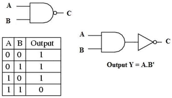
- The logic or Boolean expression for a logic NAND gate is that for Logical Addition, which is the opposite of the AND gate. The Boolean expression for a logic NAND gate is denoted by a single dot or full stop symbol, (.) with an over line or bar, ( ‾ ) over the expression to signify the NOT or logical negation of AND gate.
- The commonly used AND gate IC is 7400. It has four independent NAND gates with a standard pin configuration. The operating temperature is 70-degree Celsius.
Applications of IC 7400
- These ICs are used to design a system like theft or burglar alarms.
- These are used in freezer warning buzzer.
- These are used in theft alarms activated by light.
- These are used in an automatic watering system.
