
Introduction
Everything around us is made up of atoms and molecules. Traditionally, the behavior of materials was studied at the atomic or molecular level. However, scientific advancements revealed the existence of a scale even smaller than the molecular scale, known as the nanoscale.
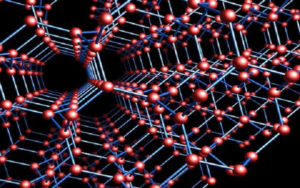
The nanoscale refers to dimensions of one billionth of a meter (1 nm = 10-9 meters). An atom is approximately 0.1 nm in size. Since atoms are the basic building blocks of matter, they can be arranged at the nanoscale to form new materials with unique properties. Nanotechnology deals with the study, manipulation, and application of materials at this scale.
What is Nanotechnology?
The term nano refers to one billionth of a meter. Nanotechnology is the field of science that focuses on the manipulation of matter at the nanoscale, typically between 1 and 100 nanometers. This scale is smaller than the wavelength of visible light.
At the nanoscale, materials exhibit different physical, chemical, and quantum properties compared to their bulk counterparts. Because of these unique characteristics, nanotechnology integrates multiple scientific disciplines such as organic chemistry, molecular biology, surface science, energy storage, semiconductor physics, molecular engineering, and microfabrication.
Basics of Nanotechnology
Nanoscale research is fascinating because it represents the stage at which individual atoms are arranged to form materials. The nanoscale lies between the atomic scale and the microscale, ranging from 1 to 100 nanometers.
At this level, the laws of quantum mechanics dominate material behavior. For example, a material that acts as an insulator at the molecular scale may behave as a semiconductor at the nanoscale. Additionally, increased surface area at this scale can alter melting points, electrical conductivity, and chemical reactivity.
Nanotechnology is often described as the science of building high-performance materials and devices from the ground up using modern tools and techniques.
Types of Nanotechnology
Nanotechnology encompasses various scientific branches that deal with matter at the nanoscale. Some of the major types include:
- Nanoengineering: Focuses on manipulating materials to develop high-performance transistors and microprocessors.
- Nanoelectronics: Involves electronic components and devices fabricated using nanotechnology.
- Nanomedicine: Deals with the development of pharmaceutical products, drug delivery systems, and medical diagnostics using nanotechnology.
Nanotechnology follows two main approaches:
- Bottom-Up Approach: Materials are constructed atom by atom or molecule by molecule, starting from basic building blocks.
- Top-Down Approach: Larger materials are reduced in size to produce nanoscale structures.
The evolution of nano mechanics, nano photonics, and nanoionics has provided a strong scientific foundation for modern nanotechnology.
Uses of Nanotechnology
Nanotechnology has found applications across multiple industries. Nanoscale materials are widely used in bulk applications to enhance performance and reduce production costs.
- Use of nanofillers to reduce the cost and improve efficiency of solar cells
- Biomedical applications such as biosensors, drug delivery systems, and tissue engineering
- Development of artificial DNA structures and study of nucleic acids
- Creation of precisely shaped molecules for advanced material synthesis
- Advanced fabrication techniques such as nanolithography and atomic layer deposition
Advantages and Disadvantages of Nanotechnology
Advantages
- Improves material strength, durability, and stability
- Enables lighter and more efficient materials
- Enhances electrical conductivity and chemical reactivity
- Leads to the development of new scientific fields and technologies
Disadvantages
- Potential environmental and health risks
- High development and implementation costs
- Uncertainty about long-term ecological impact
- Concerns regarding economic imbalance and ethical issues
Future Scope of Nanotechnology
Future research in nanotechnology is expected to focus on nanorobotics and its applications in medicine and pharmaceuticals. Scientists are exploring new nanomanufacturing tools for commercial use. Advanced nanomaterials and nano systems will be developed with the help of proposed nanomachines. Research is also underway to create materials that can be easily controlled and reversed externally.
With the advancement of nanotechnology, new interdisciplinary fields such as biotechnology and femtotechnology have emerged, highlighting the vast potential of this evolving technology.