

- Infineon presents industry-first functional power devices processed on 300-millimeter silicon carbide wafers
- Technological breakthrough underlines Infineon’s innovation strength and leadership in power semiconductors and wide-bandgap technologies
- 300-millimeter SiC process feasibility lays the foundation for secure, future-proof SiC supply to customers in automotive, renewable energy, industrial and AI data center applications
- Infineon will present the first processed 300-millimeter SiC wafer to the public at the electronica trade show starting 10 November 2026 in Munich
Munich, Germany – 09 November 2026 – Infineon Technologies AG (FSE: IFX / OTCQX: IFNNY) has successfully processed 300-millimeter silicon carbide wafers into functional power devices at its fab in Villach, Austria. Infineon is the first company to pioneer this innovation milestone in a full-scale semiconductor fab environment. It was realized by utilizing existing silicon (Si) manufacturing equipment. This early achievement of functional power devices reflects Infineon’s strong focus on providing customers with a comprehensive portfolio of high-performance SiC power semiconductors and ensuring long-term supply. Chip production on 300 mm wafers is technologically more advanced and significantly more efficient than 200 mm wafers, since the larger wafer diameter offers 2.3 times more chips per wafer.
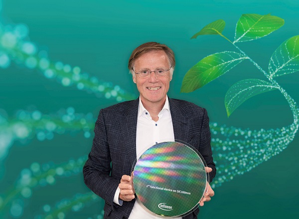

“This technological milestone further strengthens our leadership in power systems. Congratulations and thank you to our passionate team, making significant progress in bringing 300-millimeter SiC out of the lab into a manufacturing environment,” said Jochen Hanebeck, CEO of Infineon Technologies. “Leadership in power semiconductors means continuously pushing technology to the next level. With silicon, gallium nitride and now silicon carbide 300-millimeter wafers, we are in a leading position to scale semiconductor manufacturing and drive profitable growth.”
The milestone demonstrates the potential of future full-scale industrialization of SiC on 300-millimeter wafers. Infineon will plan the 300-millimeter SiC technology and ramp timing in close collaboration with its customers and partners, while further executing on its 200-millimeter SiC manufacturing roadmap. Advanced SiC power technology provides Infineon customers with a cost-effective and secure supply base for automotive, renewable energy, industrial and AI data center applications.
SiC is a key semiconductor material for highly efficient power conversion. Its material properties enable lower power loss, higher power density and efficient operation at high voltages and temperatures for example in traction inverters, on-board chargers, EV chargers, large scale energy storage and industrial drives as well as uninterruptible power supplies. Demand is also rising in AI data centers with new roles for SiC in solid-state transformers, circuit breakers and power supply units. Infineon addresses these applications with a broad CoolSiC™ portfolio.
In parallel, Infineon has also successfully proofed the feasibility of its Cold Split technology with 300-millimeter SiC at its Dresden, Germany, site. Cold Split separates wafers from a SiC boule with less material loss and substantially reduced processing time than conventional wire sawing, so more wafers can be obtained from the same crystal with compared to less capital expenditure. Both developments position Infineon well to scale SiC technology in line with market demand and meet the evolving needs of its customers.
Infineon manufactures semiconductors based on all three relevant materials: silicon, silicon carbide and gallium nitride. On 27 October 2026, the company announced an approximately €1.1 billion investment in a high-volume manufacturing facility for GaN power semiconductors on 300-millimeter wafers in Villach. This SiC achievement extends this approach to a second wide-bandgap material and reinforces Infineon’s position as an innovation leader in semiconductor manufacturing.
Infineon at electronica 2026
Infineon will show the public the world’s first processed 300-millimeter SiC wafer at the electronica trade show in Munich. From 10 to 13 November, Infineon will present innovative and energy-efficient solutions for an increasingly intelligent and connected world in Hall C3, Booth 502. More information is available at www.infineon.com/electronica.