Semiconductor for You
  • Home
  • Semiconductor News
  • Semiconductor Magazine
  • Technology
    • Automotive
    • Consumer Electronics
    • IoT
    • Test and Measurement
    • Lighting
    • Power Management
    • Wireless
    • Personal Electronics
    • Hardware & Software
    • Research
    • Medical Electronics
    • Embedded Design
    • Aerospace & Defence
    • Artificial Intelligence
  • Interview
  • Industries
  • Market
  • Knowledge Base
  • Events
  • Tools
    • Resistor Color Code Calculator
No Result
View All Result
  • Home
  • Semiconductor News
  • Semiconductor Magazine
  • Technology
    • Automotive
    • Consumer Electronics
    • IoT
    • Test and Measurement
    • Lighting
    • Power Management
    • Wireless
    • Personal Electronics
    • Hardware & Software
    • Research
    • Medical Electronics
    • Embedded Design
    • Aerospace & Defence
    • Artificial Intelligence
  • Interview
  • Industries
  • Market
  • Knowledge Base
  • Events
  • Tools
    • Resistor Color Code Calculator
No Result
View All Result
Semiconductor for You
No Result
View All Result
Home Semiconductor News

Infinitesima to commercialise powerful new methods for semiconductor device characterisation

Semiconductor For You by Semiconductor For You
January 9, 2023
in Semiconductor News
0
ADVERTISEMENT

The addition of the tomographic capability builds on the RPM technology that has already broken new ground in taking AFM from Lab to Fab with the launch of the Metron3D.

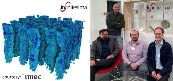
The RPM, a unique type of Atomic Force Microscope (AFM) has demonstrated disruptive potential, being used in the Metron3D metrology system to deliver in-line imaging at up to 100x the speed of conventional AFM. Using existing features of the design in new ways has enabled further innovation, providing 3D tomographic capability for semiconductor characterisation. The system uses multiple probes to generate sub-nanometre resolution 3D map of conductivity and geometry that can provide powerful insights in the development of new device architectures.

ADVERTISEMENT

Today’s semiconductor devices use complex 3D structures to achieve high density and high performance, with feature dimensions of just a few nanometres. When a device fails it can be challenging to determine the root cause, whether it’s particle contamination, dopants, or voids in the structure. The ability to generate sub-nanometre resolution 3D maps of both the device geometry and the local electrical properties enables straightforward visualisation and identification of these defect sources.

Existing tomographic techniques, such as FIB sectioning are limited in applicability due to sample damage, resolution, and measurement acquisition time. The unique capability of the RPM microscope to switch between probes whilst maintaining precise alignment enables layer removal, conductive AFM, and imaging to be fully automated.

To realise this capability, Infinitesima are extending their Joint Development Programme (JDP) with imec. Peter Jenkins, CEO of Infinitesima comments “We are very proud to be continuing our work with imec to commercialise their pioneering research”. “To continue Moore’s law there is a transition towards ever smaller and more complex 3D device structures. Current characterisation and metrology methods are reaching their limits and we need new solutions now to enable the technology of tomorrow.”

Infinitesima Ltd are leading the transition of AFM to in-line metrology. Learn more about the Metron3D and the RPM technology.


Tags: semiconductor manufacturing
Semiconductor For You

Semiconductor For You

Browse by Category

  • Aerospace and Defence
  • AI & Data Center
  • Articles
  • Automation
  • Automotive
  • Communication
  • Consumer-Electronics
  • Design & Manufacturing
  • Hardware & Software
  • Industrial Electronics
  • Interview
  • IoT
  • Knowledge Base
  • Lighting
  • Market
  • personal-electronics
  • Power Management
  • Research
  • Semiconductor Events
  • Semiconductor News
  • Sensors
  • Technology
  • Test and Measurement
  • Uncategorized
  • Wireless
Semiconductor For You

Semiconductor For You is a resource hub for electronics engineers and industrialist. With its blend of
technology features, news and new product information, Semiconductor For You keeps designers and
managers up to date with the fastest moving industry in the world.

Follow Us

Browse by Category

  • Aerospace and Defence
  • AI & Data Center
  • Articles
  • Automation
  • Automotive
  • Communication
  • Consumer-Electronics
  • Design & Manufacturing
  • Hardware & Software
  • Industrial Electronics
  • Interview
  • IoT
  • Knowledge Base
  • Lighting
  • Market
  • personal-electronics
  • Power Management
  • Research
  • Semiconductor Events
  • Semiconductor News
  • Sensors
  • Technology
  • Test and Measurement
  • Uncategorized
  • Wireless

Recent News

Description of Antenna Tuner or Antenna Tuning

Description of Antenna Tuner or Antenna Tuning

July 25, 2026
Caliber Interconnects Showcases AI-Driven Semiconductor Testing Leadership at IEEE ITC India 2026 Bengaluru, India

Caliber Interconnects Showcases AI-Driven Semiconductor Testing Leadership at IEEE ITC India 2026 Bengaluru, India

July 25, 2026
  • About
  • Advertise
  • Privacy & Policy
  • Contact

© 2026 Semiconductor For You

No Result
View All Result
  • Home
  • Semiconductor News
  • Technology
    • IoT
    • Wireless
    • Power Management
    • Automotive
    • Hardware & Software
  • Market
  • Interview
  • Knowledge Base
  • Tools
    • Resistor Color Code Calculator

© 2026 Semiconductor For You