
What is a State Variable Filter?
A State Variable Filter (SVF) is a second-order active RC filter that uses operational amplifiers (op-amps) to produce multiple frequency responses from a single circuit. It can generate three basic outputs:
- Low-Pass (LP) output
- High-Pass (HP) output
- Band-Pass (BP) output
An additional summing amplifier can be added to generate a fourth output: a Notch or Band-Stop response. A basic state variable filter consists of three op-amp stages: two integrators and one summing amplifier. The circuit uses feedback between these stages to control its frequency response. One of the main advantages of a state variable filter is that its centre frequency and quality factor (Q) can be adjusted independently in a properly designed circuit.

Working Principle of a State Variable Filter
A state variable filter uses two op-amp integrators and a summing amplifier to produce different filter responses. The summing amplifier combines the input signal with feedback signals from the other stages. Its output produces the high-pass response, which is then passed through the first integrator. The first integrator produces the band-pass response. This output becomes the input to the second integrator, which produces the low-pass response.
Therefore, the three outputs are obtained as follows:
- High-Pass Output (VHP): Produced by the summing amplifier.
- Band-Pass Output (VBP): Produced by the first integrator.
- Low-Pass Output (VLP): Produced by the second integrator.
An additional op-amp summing stage can combine the high-pass and low-pass outputs to produce a notch filter response.
Block Diagram of a State Variable Filter
The basic state variable filter has three main op-amp stages. Each stage provides a different output response.
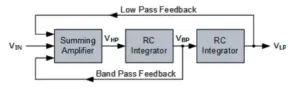
The block diagram includes:
- A summing amplifier
- First op-amp integrator
- Second op-amp integrator
- Feedback connections between the stages
The summing amplifier receives the input signal and feedback signals. The resulting high-pass output is integrated to obtain the band-pass output. The second integration produces the low-pass output.
Op-Amp Integrator in a State Variable Filter
An op-amp integrator is an important part of a state variable filter. It uses a capacitor in its feedback path to perform integration. The output voltage of an ideal inverting integrator is proportional to the time integral of its input voltage.
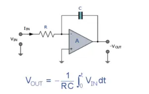
The transfer function of an ideal inverting integrator is:
Vout/Vin = -1/(sRC)
Where:
- Vout = Output voltage
- Vin = Input voltage
- R = Input resistance
- C = Feedback capacitance
- s = Complex frequency variable
The negative sign indicates an inversion of the output signal. In a state variable filter, the output of the first integrator becomes the input of the second integrator. This arrangement produces the band-pass and low-pass responses.
Summing Amplifier in a State Variable Filter
The summing amplifier is another important part of the state variable filter. It combines the input signal with feedback signals from the integrator stages. In the basic design, the summing amplifier acts as an adder-subtractor circuit. It combines the input voltage, band-pass output and low-pass output according to the selected resistor network. This feedback arrangement controls the filter’s damping and frequency response.
Frequency Responses of a State Variable Filter
A state variable filter can produce three different frequency responses from the same circuit.
1. Low-Pass Filter Output
A low-pass output allows low-frequency signals to pass while reducing high-frequency signals. Its output is obtained from the second op-amp integrator.
2. High-Pass Filter Output
A high-pass output allows high-frequency signals to pass while reducing low-frequency signals. It is produced by the summing amplifier.
3. Band-Pass Filter Output
A band-pass output allows a selected range of frequencies to pass while reducing frequencies below and above that range. It is obtained from the first op-amp integrator. The band-pass response is especially useful when a narrow range of frequencies needs to be selected.
Corner Frequency of a State Variable Filter
The corner frequency, also called the natural frequency, determines the frequency around which the filter operates. For two identical integrator stages having the same resistance and capacitance, the natural frequency is:
f0 = 1/(2πRC)
Where:
- f0 = Natural frequency in hertz
- R = Integrator resistance in ohms
- C = Integrator capacitance in farads
The corner frequency can be adjusted by changing either the resistor or capacitor value.
In a properly designed state variable filter, the frequency can be adjusted without significantly changing the Q factor.
Quality Factor (Q) of a State Variable Filter
The quality factor, represented by Q, describes the selectivity or sharpness of the band-pass response. A higher Q value produces a narrower bandwidth and a sharper response around the centre frequency. A lower Q value produces a wider bandwidth.
For a band-pass filter:
Q = f0/BW
Where:
- Q = Quality factor
- f0 = Centre frequency
- BW = Bandwidth
The bandwidth is the difference between the upper and lower -3 dB frequencies.
For a standard second-order response, the damping ratio (ζ) and quality factor are related by:
ζ = 1/(2Q)
A higher Q value means lower damping and greater selectivity.
State Variable Filter Design Example
Consider a state variable filter with the following specifications:
- Natural frequency = 1 kHz
- Quality factor (Q) = 10
- Equal resistance values in both integrator stages
- Equal capacitance values in both integrator stages
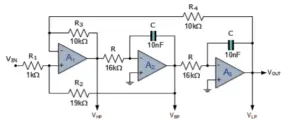
Assume a suitable capacitor value of 10 nF.
The natural frequency equation is:
f0 = 1/(2πRC)
Rearranging to calculate resistance:
R = 1/(2πf0C)
Substituting the values:
R = 1/(2 × π × 1000 × 10 × 10-9)
R ≈ 15.9 kΩ
Therefore, the selected component values are:
- C = 10 nF
- R ≈ 15.9 kΩ (approximately 16 kΩ)
The remaining resistor values must be calculated from the specific circuit topology and its summing-amplifier equations. The complete gain calculation cannot be reproduced from the supplied text because the required equations are missing.
Notch Filter Design Using a State Variable Filter
A notch filter is also known as a band-stop filter. It reduces or rejects a particular frequency while allowing frequencies outside that range to pass. A state variable filter can generate a notch response by adding another op-amp summing amplifier to the basic circuit.
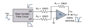
The additional amplifier combines the low-pass output (VLP) and high-pass output (VHP). Their combined response produces a notch around the centre frequency. The notch frequency corresponds to the centre frequency of the band-pass response.
Controlling the Notch Depth
The depth of the notch can be adjusted by modifying the signals supplied to the additional summing amplifier. The basic notch circuit uses the low-pass and high-pass outputs. The band-pass output (VBP) or the original input signal (VIN) can also be included to provide additional control over the notch response.
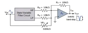
The selected feedback and resistor arrangement determines the depth and shape of the notch. It is important to note that the Q factor controls the bandwidth and selectivity of the notch. It does not directly determine the depth of the notch.
Advantages of a State Variable Filter
- It can produce low-pass, high-pass and band-pass outputs from a single circuit.
- A notch filter output can be obtained by adding another summing amplifier.
- The centre frequency and Q factor can be adjusted independently in a properly designed circuit.
- It provides good frequency selectivity.
- It is suitable for applications that require adjustable filter responses.
- Its frequency response can be tuned by changing the integrator resistor or capacitor values.
Applications of State Variable Filters
State variable filters are used in several electronic applications, including:
- Audio signal processing
- Frequency selection circuits
- Communication systems
- Electronic instrumentation
- Active filter circuits
- Signal conditioning systems
- Adjustable band-pass filter applications
Conclusion
A State Variable Filter is a second-order active RC filter that uses operational amplifiers, integrators and feedback networks to produce multiple frequency responses. Its main advantage is that it can provide low-pass, high-pass and band-pass outputs from a single circuit. By adding another summing amplifier, a notch filter output can also be obtained. Because of its adjustable centre frequency and Q factor, the state variable filter is useful in audio processing, communication systems and other electronic applications.