

By Thomas Apel

Using High‑Impedance States to Expand LED Drive Capacity
Embedded designs often use LEDs to show status, errors, or operating modes. As products become smaller, the number of available GPIO pins is often limited. Assigning one pin to each LED is simple, but this approach does not scale well in compact or cost sensitive systems.

Tri-state multiplexing provides a practical alternative. Each GPIO output can operate in three states: logic high, logic low, or high impedance. By carefully controlling these states, a small number of GPIO lines can drive a much larger number of LEDs. With N tri-state capable outputs, up to N times N minus one LEDs can be controlled. For example, four outputs are sufficient to drive twelve LEDs.
This article explains the principles of tri-state multiplexing and the logic needed to apply it safely. As a practical illustration, the technique is implemented using an SLG46811 GreenPAK device. This example shows how twelve LEDs can be controlled using only four GPIO pins. A complete design file is provided so readers can study the circuit and adapt the method to their own designs using Go Configure Software Hub.
How Tri-State Multiplexing Works
In a tri-state multiplexed LED network, each LED is connected between a unique pair of GPIO lines with opposite polarity. At any moment, only two outputs are actively driven. One output sources current and the other sinks current. All remaining outputs are placed in a high impedance state.
This arrangement creates a single, well defined current path, so only the selected LED turns on. All other LEDs remain off because at least one side of their connection is floating. Unlike traditional row and column matrices, this method does not require dedicated rows, columns, or external driver circuits.
To make multiple LEDs appear on at the same time, the control logic rapidly switches between LED selections. If the refresh rate is high enough, the human eye perceives steady illumination.
Example Matrix Using Four Outputs
A four-output tri-state matrix connects each GPIO to every other GPIO through an LED and a current limiting resistor. Each GPIO also includes its own resistor. This creates a compact structure where each LED corresponds to a unique source and sink pairing.
Tri-state multiplexing (tri-state signaling, charlieplexing) is a technique that makes it possible to drive a number of LEDs with fewer I/O pins than are required with a traditional multiplexed matrix (or using one output pin per LED). With N output pins, it is possible to drive up to N * (N – 1) LEDs. Thus, 2 LEDs can be driven by 2 GPIOs, 6 LEDs by 3 GPIOs, or 12 LEDs by 4 GPIOs, and so on.
This application note demonstrates how a SLG46811 device can be used to drive 12 LEDs using only 4 GPIOs.
Two operating modes are supported, with the illumination of LEDs being controlled either by a sequence configured in the extended pattern generator (EPG), or by input pins.
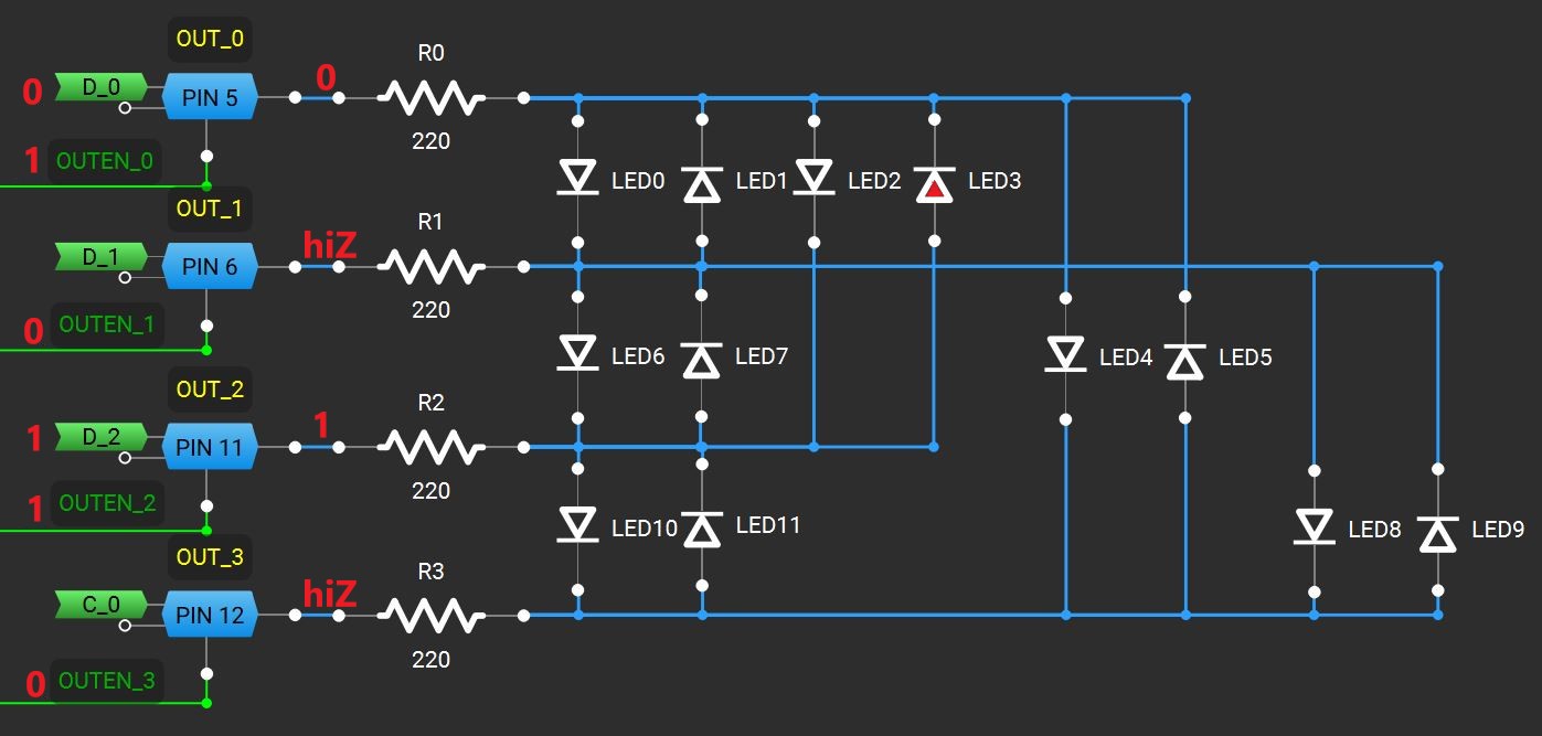
Figure 1 shows the tri-state multiplexing matrix for 4 GPIOs driving 12 LEDs. Each GPIO is connected to the LED matrix via a corresponding current-limiting serial resistor, and each GPIO is connected to every other GPIO via one path: resistor – LED in forward direction – resistor.
Some of the GreenPAK GPIOs (device dependent, please see datasheet) can be used as digital outputs that dynamically can be switched between driving either a 0 (low), 1 (high) or Hi-Z (tri-state).
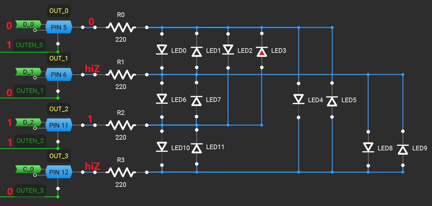
The following example (Figure 1) shows how to light up LED3 with the design shown in Figure 2.
A current flow is required from PIN11 through R2 to LED3 and R0 to PIN5, so the GPIO connected to PIN11 has to drive a 1, the GPIO connected to PIN5 has to drive a 0, and the other two GPIOs are to be set to Hi-Z.
This is achieved by enabling the outputs of the GPIOs on PIN5 and PIN11 (OUTEN_0 = 1, OUTEN_2 = 1) while disabling the other two GPIOs (OUTEN_1 = 0, OUTEN_3 = 0); the IN pin for the GPIO connected to PIN5 has to be set to 0, and the IN pin for PIN11 has to be set to 1. The logical values for the other two IN pins are don’t care.
GreenPAK Design Overview
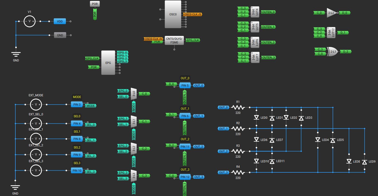
The design consists of:
- 4 GPIOs used as outputs which are switched between Hi-Z, high, or low output,
- the generation of the EPG clock with a frequency of 1 Hz
- the extended pattern generator (EPG)
- 5 GPIOs used as inputs (4 inputs for controlling the LED pattern, and 1 input for switching between the EPG and the non-EPG mode)
- a multiplexer to select between the EPG output and the 4 input pins for LED selection
- a decode logic to drive the output data and output enable signal for each of the 4 GPIOs used
In the bottom right corner of the schematic, the tri-state signaling LED matrix connected to the 4 outputs is also included.
EPG Clock Generation
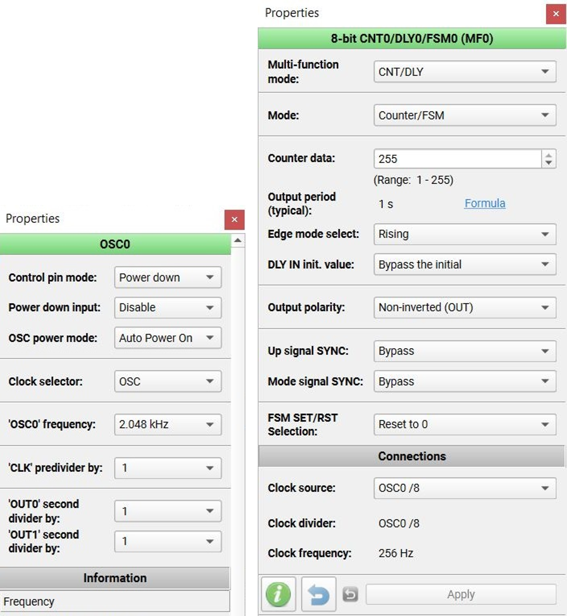
To generate a clock with a cycle time of 1 sec, the 2.048 kHz oscillator is used in combination with a clock counter (8-bit CNT0/DLY0/FSM0). The OSC0 output OSC0/8 is used as the input for the counter that outputs the EPG clock with a period of 1 second (typ). See the configuration of the properties in Figure 3.
Extended Pattern Generator
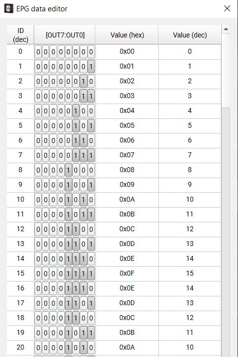
The EPG offers 92 entries with 8 bits each, with the lower 4 bits of each entry used to select a single LED.
EPG data [3:0] = 0000 will select LED0, 0001 will select LED1, …, 1011 will select LED11; the values from 1100 to 1111 are unused, and no LED will be lit.
The EPG is connected to the power-on reset (POR); starting with entry 0, with every EPG clock the EPG will present data from entry 0, 1, 2, .. 91 on its outputs and start from entry 0 again.
Figure 4 shows the properties window for the EPG (manual EPG data editor), the sequence shown here will sequentially light up LED0 through LED11 and back, including pattern 1100 to 1111 that will not select any LEDs. Other entries in the EPG data (not shown here) in this design includes other sequences such as LED0, LED2, LED4, and LED1, LED3, LED5, or LED pattern sequences starting from both ends to the middle, and so on.
LED Pattern Selection from EPG or External Inputs
The operating mode (LED pattern selected either by the EPG or external inputs) is selected via GPIO3 (MODE). When MODE input is 1, the LED pattern is controlled by input SEL[3:0] (GPIO pins 10, 9, 8 and 4) instead of EPG[3:0].
In the GPIO properties window, a 1 MΩ pulldown is selected for all five inputs, so EPG mode is selected by default if no external inputs are connected to these GPIOs.
Four 2:1 multiplexers controlled by the MODE pin are used to select between the external inputs and the EPG data for the LED pattern.
GPIO Output Control
Table 1 below details the control logic requirements for the GPIO outputs driving the LEDs.
The first column contains the possible values from the multiplexer outputs C[3:0]. The second column shows the required current flow to light up the corresponding LED. The third column shows the required GPIO output states. Columns four (orange) and five (grey) show the required control signals OUT_EN connected to each GPIO pin OE, and D connected to GPIO pin IN). A ‘-‘ in column four represents a “don’t care” value, while in column six (green), the ‘-‘ entries are replaced by either ‘0’ or ‘1’ for control logic optimization.
The first row shows the selection for LED0, which requires a current flow from OUT_0 to OUT_1 (see second column). The outputs must be enabled for OUT_0 and OUT_1 (see third column), and OUT_0 must be high, while OUT_1 must be low (see fourth/fifth column).
The required values for D[0] are identical to C[0], and the values for D[3] are identical to the inverted values of C[0]. The other control signals are dependent on two to four bits of C[3:0] and can easily be implemented via the properties windows of the 2-bit to 4-bit LUTs using the table.
Table 1: GPIO output control
| C[3:0] | LED + – | OUT[3:0] | OUT_EN[3:0] | D[3:0] | D[3:0] | |||||||||
| 0000 | 0 → 1 | Z Z 0 1 | 0 | 0 | 1 | 1 | – | – | 0 | 1 | 0 | 0 | 0 | 1 |
| 0001 | 1 → 0 | Z Z 1 0 | 0 | 0 | 1 | 1 | – | – | 1 | 0 | 1 | 1 | 1 | 0 |
| 0010 | 0 → 2 | Z 0 Z 1 | 0 | 1 | 0 | 1 | – | 0 | – | 1 | 0 | 0 | 0 | 1 |
| 0011 | 2 → 0 | Z 1 Z 0 | 0 | 1 | 0 | 1 | – | 1 | – | 0 | 1 | 1 | 1 | 0 |
| 0100 | 0 → 3 | 0 Z Z 1 | 1 | 0 | 0 | 1 | 0 | – | – | 1 | 0 | 0 | 1 | 1 |
| 0101 | 3 → 0 | 1 Z Z 0 | 1 | 0 | 0 | 1 | 1 | – | – | 0 | 1 | 1 | 0 | 0 |
| 0110 | 1 → 2 | Z 0 1 Z | 0 | 1 | 1 | 0 | – | 0 | 1 | – | 0 | 0 | 1 | 1 |
| 0111 | 2 → 1 | Z 1 0 Z | 0 | 1 | 1 | 0 | – | 1 | 0 | – | 1 | 1 | 0 | 0 |
| 1000 | 1 → 3 | 0 Z 1 Z | 1 | 0 | 1 | 0 | 0 | – | 1 | – | 0 | 1 | 1 | 1 |
| 1001 | 3 → 1 | 1 Z 0 Z | 1 | 0 | 1 | 0 | 1 | – | 0 | – | 1 | 0 | 0 | 0 |
| 1010 | 2 → 3 | 0 1 Z Z | 1 | 1 | 0 | 0 | 0 | 1 | – | – | 0 | 1 | 1 | 1 |
| 1011 | 3 → 2 | 1 0 Z Z | 1 | 1 | 0 | 0 | 1 | 0 | – | – | 1 | 0 | 0 | 0 |
| 1100 | — | Z Z Z Z | 0 | 0 | 0 | 0 | – | – | – | – | 0 | 1 | 1 | 1 |
| 1101 | — | Z Z Z Z | 0 | 0 | 0 | 0 | – | – | – | – | 1 | 0 | 0 | 0 |
| 1110 | — | Z Z Z Z | 0 | 0 | 0 | 0 | – | – | – | – | 0 | 1 | 1 | 1 |
| 1111 | — | Z Z Z Z | 0 | 0 | 0 | 0 | – | – | – | – | 1 | 0 | 0 | 0 |
Test
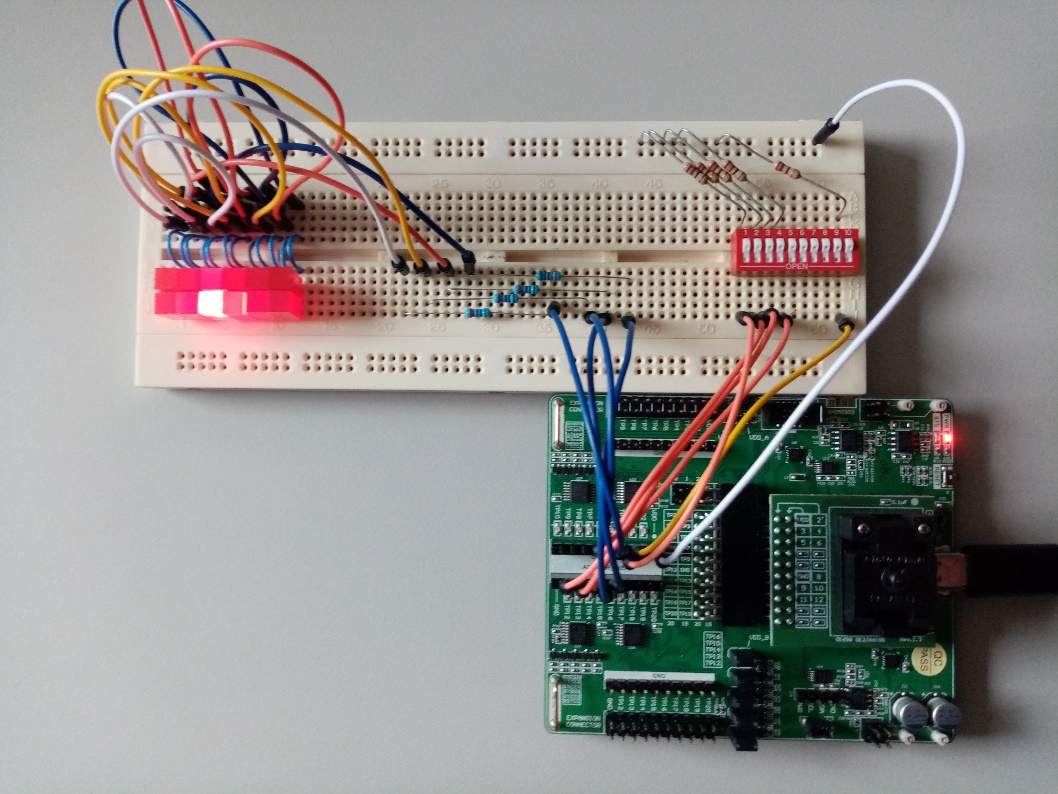
After verifying correct behavior of the design in both EPG (MODE = 0) and non-EPG modes (MODE = 1) in simulation, the SLG46811 device is programmed using the GreenPAK Lite Development board and the SLG46811 socket adapter.
On a breadboard connected to the SLG46811 GPIOs via the DIP adapter connector, the tri-state multiplexing LED matrix is implemented with its wire connections and the four current-limiting resistors.
On the right side of the breadboard, a DIP-switch is used to control the MODE and SEL[3:0] inputs. Switching one of the five switches to ON will connect the corresponding GPIO to VDD via a low-ohm resistor (220 Ω), thus driving the GPIO input to high.
Table 2 shows the mapping of the SLG46811 device’s GPIOs to the pins and test points (TPs) on the DIP adapter connector that are connected to the LED matrix and the DIP switch on the breadboard:
Table 2: Mapping of SLG46811 device GPIOs to pins and TPs on DIP adapter
| SLG46811 device | DIP adapter | ||||
| Pin # | Pin Name | Function | I/O | Pin # | TP |
| 1 | VDD | VDD | VDD | 1 | VDD |
| 2 | PIN 2 | N/C | — | 2 | |
| 3 | PIN 3 | MODE | IN | 3 | TP3 |
| 4 | PIN 4 | SEL_0 | IN | 4 | TP4 |
| 5 | PIN 5 | OUT_0 | OUT | 5 | TP5 |
| 6 | PIN 6 | OUT_1 | OUT | 6 | TP6 |
| 7 | GND | GND | GND | 7 | |
| 8 | PIN 8 | SEL_1 | IN | 8 | TP12 |
| 9 | PIN 9 | SEL_2 | IN | 9 | TP13 |
| 10 | PIN 10 | SEL_3 | IN | 10 | TP14 |
| 11 | PIN 11 | OUT_2 | OUT | 11 | TP15 |
| 12 | PIN 12 | OUT_3 | OUT | 12 | TP16 |
Table 3shows the decoding of the SEL inputs (DIP switch) to LED pattern in case the external mode is selected (MODE = 1):
Table 3: Decoding the SEL[3:0] inputs to the LED pattern
| PIN 10 / TP14 | PIN 9 / TP13 | PIN 8 / TP12 | PIN 4 / TP4 | LED pattern |
| SEL_3 | SEL_2 | SEL_1 | SEL_0 | |
| 0 | 0 | 0 | 0 | LED0 on |
| 0 | 0 | 0 | 1 | LED1 on |
| 0 | 0 | 1 | 0 | LED2 on |
| 0 | 0 | 1 | 1 | LED3 on |
| 0 | 1 | 0 | 0 | LED4 on |
| 0 | 1 | 0 | 1 | LED5 on |
| 0 | 1 | 1 | 0 | LED6 on |
| 0 | 1 | 1 | 1 | LED7 on |
| 1 | 0 | 0 | 0 | LED8 on |
| 1 | 0 | 0 | 1 | LED9 on |
| 1 | 0 | 1 | 0 | LED10 on |
| 1 | 0 | 1 | 1 | LED11 on |
| 1 | 1 | 0 | 0 | no LED on |
| 1 | 1 | 0 | 1 | no LED on |
| 1 | 1 | 1 | 0 | no LED on |
| 1 | 1 | 1 | 1 | no LED on |
The photo below (Figure 5) shows the development board and the breadboard, with the LED numbers and the DIP switches controlling the inputs MODE and SEL[3:0].
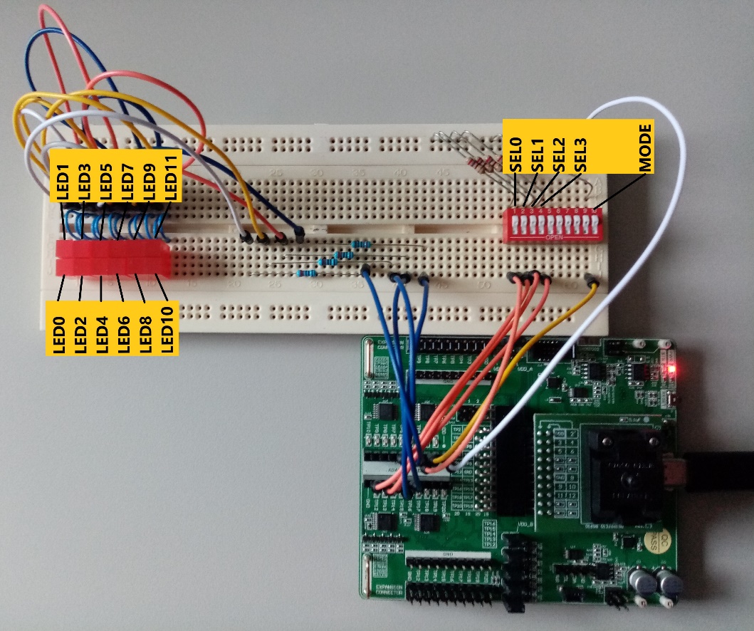
Figure 6 shows the design in non-EPG mode (MODE set to 1, SEL set to 0000, LED0 is lit up):
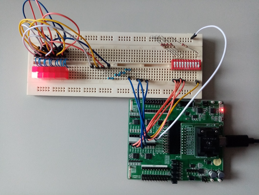
Figure 7 shows the design in non-EPG mode (MODE set to 1, SEL set to 1011, LED11 is lit up):
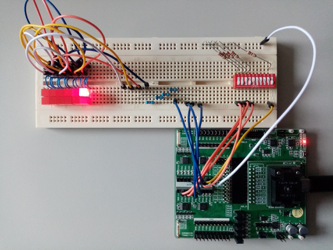
Figure 8 shows the design in EPG mode (MODE set to 0; at the time the photo was taken, LED4 was selected by the EPG output):
Conclusion
The presented implementation shows an efficient method for controlling 12 LEDs using only four GPIOs by utilizing the configurable logic resources of the GreenPAK SLG46811. The design combines internal pattern generation with optional external control, enabling flexible operation while maintaining a compact hardware footprint. It serves as an example of how configurable mixed-signal devices can reduce component count and simplify LED control in resource-constrained systems.