• Home
  • About Us
  • Contact Us
Semiconductor for You
  • Home
  • Semiconductor News
  • Magazine
  • Technology
    • Automotive
    • Consumer Electronics
    • IoT
    • Lighting
    • Power Management
    • Wireless
    • Personal Electronics
    • Hardware & Software
    • Research
    • Medical Electronics
    • Embedded Design
    • Aerospace & Defence
    • Artificial Intelligence
  • DIY Projects
  • Market
  • Industries
    • Renesas Electronics
  • Knowledge Base
  • Events
  • Tools
    • Resistor Color Code Calculator
No Result
View All Result
Semiconductor for You
No Result
View All Result
Home Articles

What is depletion region?

Semiconductor For You by Semiconductor For You
June 1, 2021
in Articles
0
ADVERTISEMENT
  • Difference in concentration of charge carrier in the two sections of P-N junction.
  • The electrons from N-region diffuse through the junction into p-region and the hole from p region diffuse into N-region.
  • Neutrality of both N and P-type semiconductors is disturbed, a layer of negative charged ions appear near the junction in the p-crystal and layer of positive ions appears near the junction in N-crystal.
  • The solid circles on the right of the junction represent the available electrons from the n-type dopant. Near the junction, electrons diffuse across to combine with holes, creating a “depletion region”.

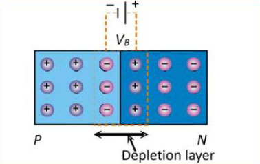
  • Depletion region is a region near the p-n junction where flow of charge carriers (free electrons and holes) is reduced over a given period and finally results in zero charge carriers.
Content Protection by DMCA.com
Tags: P-N junctionSemiconductors
Semiconductor For You

Semiconductor For You

Browse by Category

  • Aerospace and Defence
  • Articles
  • Automotive
  • Consumer-Electronics
  • Hardware & Software
  • Interview
  • IoT
  • Knowledge Base
  • Lighting
  • Market
  • personal-electronics
  • Power Management
  • Research
  • Semiconductor Events
  • Semiconductor News
  • Technology
  • Wireless
Semiconductor for You

Semiconductor For You is a resource hub for electronics engineers and industrialist. With its blend of
technology features, news and new product information, Semiconductor For You keeps designers and
managers up to date with the fastest moving industry in the world.

Follow Us

Browse by Category

  • Aerospace and Defence
  • Articles
  • Automotive
  • Consumer-Electronics
  • Hardware & Software
  • Interview
  • IoT
  • Knowledge Base
  • Lighting
  • Market
  • personal-electronics
  • Power Management
  • Research
  • Semiconductor Events
  • Semiconductor News
  • Technology
  • Wireless

Recent News

SEMI and India Semiconductor Mission (ISM) Announce the Opening of Visitor Registrations for SEMICON® India 2025

July 11, 2025
New QSMP-25 solder-down module features next-gen STM32 MPU to enable secure edge AI in Industry 4.0 applications

New QSMP-25 solder-down module features next-gen STM32 MPU to enable secure edge AI in Industry 4.0 applications

July 11, 2025
  • About
  • Advertise
  • Privacy & Policy
  • Contact

© 2022 Semiconductor For You

No Result
View All Result
  • Home
  • Semiconductor News
  • Technology
    • IoT
    • Wireless
    • Power Management
    • Automotive
    • Hardware & Software
  • Market
  • Knowledge Base
  • Tools
    • Resistor Color Code Calculator

© 2022 Semiconductor For You